No products in the cart.
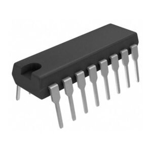
CD 4013 IC Dual D-Type Flip-Flop


Roll over image to zoom in
EGP25.00
CD 4013 IC Dual D-Type Flip-Flop
4013 Pinout Description
Pin No Pin Symbol Name Description
1,13 1Q/2Q Output Output Pin of the Flip Flop
2,12 1Q’(bar)/2Q’(bar) Complementary Output The inverted output pin of Flip Flop
3, 11 1CP/2CP Clock Input Pin These pins must be provided with a clock pulse for the flip-flop
4,10 1CD/2CD Clear Data Resets the flip-flop by clearing its memory
5,9 1D/2D Data Input Pin Input pin of the Flip Flop
6,8 1SD/2SD Set-direct Input Another Input pin for Flip Flop
7 Vss Ground Connected to the ground of the system
14 Vdd/Vcc Supply Voltage Powers the IC typically with 5V
Specifications
Product Attribute Attribute Value
Product Category: Flip-Flops
Number of Circuits: 2
Logic Type: D-Type Flip-Flop
Polarity: Inverting/Non-Inverting
Input Type: CMOS
Output Type: CMOS
Propagation Delay Time: 300 ns
High-Level Output Current: – 1.5 mA
Low-Level Output Current: 1.5 mA
Supply Voltage – Min: 3 V
Supply Voltage – Max: 18 V
Minimum Operating Temperature: – 55 C
Maximum Operating Temperature: + 125 C
Mounting Style: Through Hole
Package/Case: PDIP-14
Packaging: Tube
Function: Dual CMOS
Number of Channels: 2
Number of Input Lines: 1
Number of Output Lines: 1
Operating Supply Voltage: 10 V
Operating Temperature Range: – 55 C to + 125 C
Quiescent Current: 20 uA
Reset Type: Set, Reset
How to use D Flip-Flop (4013)?
Using a Flip-Flop is pretty straightforward. Simply power the IC using the 7th and 14th pins. As told earlier each flip-flop operates independently, just connect the input signals 5 and 6 for using the 1st flip-flop and you will get the output at pins 1 and 2. Pin 3 should be provided with a clock source normally a PWM signal from an MCU or 555 timer is used. The pin can be used to clear the data and reset the flip-flop by making it high. The complete working of the Flip flop can be understood by looking at the function table below. The symbol “X” indicates don’t care and the up-arrow indicates the rising edge of the signal.
Flip Flop Working
You can also simulate the IC to check if it would work as desired. Here I have used logic state and logic bits to view if the IC functions as it is supposed to, but you can replace them with the actual circuitry of your application to check if it would suit your needs. The gif file shown below can be verified with the truth table given above to make sure that the IC works as desired.
D Flip-Flop
Additional information
| Title | Default Title |
|---|